The process of making chips
(Amplify the chip by 100,000 times. These things smaller than viruses are transistors, and hundreds of billions of transistors form a chip)
1. Raw material preparation
200 kg single crystal silicon rod.
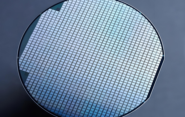
Then cut into silicon wafers with a thickness of less than one millimeter, polish the smooth surface, and the fineness reaches 0.1 nanometers to form the raw material of the chip - wafer.
2. Wafer transport and processing
230 chips (each chip is only the size of a fingernail) require thousands of processes, and the core steps are completed in a lithography machine.
3. Lithography machine: the core of nano-level "sculpting"
Volume comparison: The lithography machine is equivalent to superimposing two buses, and the internal integration of high-precision optical and mechanical systems.
How it works:
Engineers design transistor circuit diagrams and print them onto photomasks (line fineness < 1/10000 of hair).
Engraving circuits using extreme ultraviolet light (EUV):
High-intensity laser light is emitted in a vacuum environment (15 times the intensity of metal cutting laser light).
The laser hits the molten tin droplets, vaporizes to create plasma and releases extreme ultraviolet light.
The mirror collects EUV light and projects it to the wafer surface (difficulty comparable to "moon laser accurately hits the fingers of the earth.").
Environmental requirements: The photolithography machine maintains a vacuum (air will absorb EUV light), so it is extremely difficult to manufacture.
4. Circuit engraving process
Photoresist coating: The wafer surface is covered with photoresist (sensitive to ordinary light, and the workshop needs to be protected by yellow light).
Pattern transfer: EUV light irradiates the wafer through the photomask, and the photoresist falls off to form a circuit pattern.
Etching and copper clad:
Corrosion of unprotected areas forms silicon trenches.
Deposit the copper layer and grind it to prevent short circuits (the single-layer line thickness is only a few nanometers).
5. Multi-layer superposition: building a three-dimensional circuit
More than 100 times, more than 100 layers of lines are superimposed, and interlayer conductivity is achieved through metal interconnection.
Cleanliness requirements:
The workshop is equipped with a 12,000-ton fresh air system, which is breathed every 2 minutes (a hundred times cleaner than the operating room).
Flush the wafer with ultrapure water to avoid short circuits caused by dust.
6. Defect Management and Chip Grading
Defect Tolerance: Some kernel defects only reduce performance and do not affect use.
Level classification:
i9 chip: the fewest defects, the strongest performance, the highest price.
i3 chip: many defects, moderate performance, affordable price.
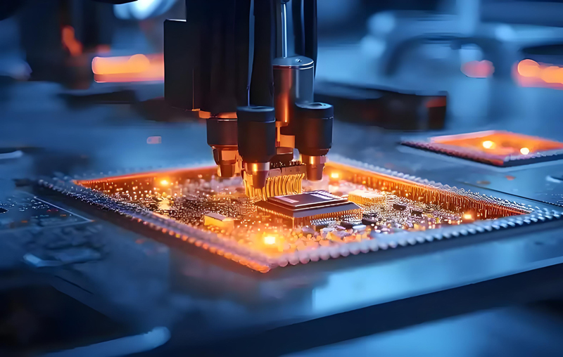
7. Packaging and testing
After two months of processing, the CPU was finally manufactured.
Conclusion
Chip manufacturing is the pinnacle of material science, optics, precision machinery and clean technology. From sand particles to nano-scale circuits, every process embodies human pursuit of the ultimate. In the future, with the iteration of technology, the transistor density and performance on the chip will continue to break through imagination!