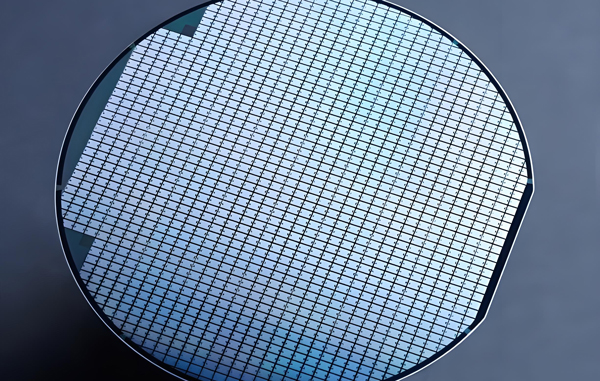
The semiconductor film process is an indispensable basic link in chip manufacturing. Its essence is to accurately deposit or grow nano-scale films on the wafer surface, giving the chip conductive, insulating or protective functions. These films are usually between a few angstroms and microns thick, but determine the transistor's performance, interconnect reliability, and device life. Whether it is the gate dielectric layer of the logic chip, the capacitance structure of the memory, or the passivation protection film of the power semiconductor, the thin film process runs through every key stage of chip manufacturing.
Mainstream technical routes and principles
Chemical Vapor Deposition (CVD)
A solid film is formed on the wafer surface by chemical reaction of the gaseous precursor at high temperature or plasma environment. For example, materials such as polycrystalline silicon, silicon nitride and silicon dioxide can all be deposited with high quality through CVD.
Atmospheric pressure CVD (APCVD): Suitable for thick film growth, such as epitaxial silicon layer;
Low-voltage CVD (LPCVD): used to prepare a uniform silicon nitride mask layer;
Plasma-enhanced CVD (PECVD): It can deposit a dielectric layer at low temperatures to reduce thermal damage to the chip.
The advantage of CVD lies in its excellent step coverage, which is especially suitable for complex three-dimensional structures, but its reactive gas management and by-product control are technical difficulties.
Physical Vapor Deposition (PVD)
Transfer target atoms to the wafer surface by physical means (such as sputtering, evaporation).
Magnetically controlled sputtering: mainstream PVD technology uses plasma to bombard metal targets, and the sputtered atoms are deposited into conductive films, which are widely used in aluminum and copper interconnection processes;
Electron beam evaporation: The target material (such as gold and titanium) is melted by high-energy electron beams to form a high-purity film.
The PVD deposition rate is fast and the purity is controllable, but the step coverage is poor, so it needs to be optimized in combination with subsequent process.
Atomic layer deposition (ALD)
By alternately passing into different precursors, a self-limiting reaction occurs on the surface, and atomic uniform films are grown layer by layer. For example:
High-k gate dielectric materials (such as HfO?) and Al?O?/TiO? stacking of DRAM capacitors both rely on ALD technology.
The thickness control accuracy of ALD can reach a single atomic layer (±0.1nm), but the deposition speed is slow and the cost is high, and it is usually only used for critical functional layers.
Key equipment and technical challenges
CVD equipment
Thermal wall CVD furnace: used to mass-produce polycrystalline silicon or oxides, and the temperature uniformity must be controlled within ±2℃;
Monolithic PECVD equipment: Integrated RF plasma source, supporting low damage deposition of 12-inch wafers, but gas distribution uniformity and plasma stability are core challenges.
PVD equipment
Magnetically controlled sputtering equipment: improve the target utilization rate to more than 70% by optimizing the magnetic field distribution, but the processing accuracy and low-damage sputtering of large-size copper targets still need to be made breakthroughs;
Ionized PVD (I-PVD): Improve step coverage by ionizing target atoms, and has become the standard technology for advanced processes below 5nm.
ALD equipment
Thermal ALD and plasma ALD: The former produces dense films at 200~350°C, while the latter supports low-temperature deposition (<100°C) to be compatible with sensitive materials;
Space ALD technology: Increase deposition speed through the relative motion of wafers and nozzles. For example, ASM's Pulsar? system has been mass-produced.
Application scenarios and typical cases
Logic chip: The high-k metal gate structure depends on ALD-deposited HfO? and the TiN film prepared by PVD; the copper interconnection process requires the combination of PVD's TaN barrier layer and CVD's copper seed layer.
DRAM capacitor: Al?O? and TiO? are alternately stacked by ALD to achieve high-density charge storage.
Power semiconductor: PECVD-grown Si?N? passivation layer prevents moisture from eroding the surface of the IGBT chip.
Advanced Package: Rewiring layer (RDL) and through silicon (TSV) integrated polyimide dielectric layer with copper conductors.
Domestic and foreign gaps and breakthrough paths
Equipment performance: The ALD equipment of the leading international enterprises has achieved thickness uniformity of ±1% of 300mm wafers, while the uniformity of domestic equipment on 200mm wafers is still ±3%;
Materials and components: In terms of PVD target utilization, the utilization rate of domestic copper targets is only 50%~60%, which is lower than the international level 75%; core components such as high-purity precursor materials (such as WF?, HfCl?) and vacuum pumps still rely on imports;
Process integration: TSMC's 3nm process uses ALD HfZrO? gate dielectric, while the domestic 28nm process is still dominated by traditional CVD.
Breakthrough direction:
Conquer the domestic production of high-purity quartz tubes, target materials and precursors;
Develop an AI-driven process control system to improve film uniformity;
Layout and integration technology of wide bandgap semiconductors (such as GaN, SiC).
Future trends: precision and multi-dimensional expansion
Atomic precision manufacturing: Single-layer deposition of two-dimensional materials (such as MoS?) and sub-nano interface control technology will promote the birth of new devices;
Wide bandgap semiconductors: demand for gallium nitride epitaxial layer (MOCVD) and gallium oxide channel layer (HVPE) is growing, driving the research and development of special equipment;
Green manufacturing: replace highly toxic precursors (such as replacing WF? with organic tungsten compounds), and strengthen exhaust gas recovery;
Intelligent: Through machine learning, machine learning optimizes deposition parameters in real time to increase process stability by more than 20%.
Conclusion
Semiconductor thin film process is a bridge connecting materials science and chip performance. From the chemical reaction of CVD to the atomic manipulation of ALD, the deposition of each layer of film is the ultimate pursuit of accuracy and efficiency. Breaking through the collaborative bottleneck of equipment, materials and processes will become a key battle for China's semiconductor industry to climb the technological peak.


