The following is the optimized layout text, which enhances the sense of layering through segmentation, marking and indentation, while retaining all original information:
The development of semiconductors has led a technological revolution. From early transistor radios to modern ultra-large-scale integrated circuits, the advancement of semiconductors has promoted the development of the entire information age. However, semiconductors are not just the driving force of technology, they are also an important window for us to understand the world. By delving into semiconductors, we can better understand the behavior of matter and how we can use this knowledge to create the technology that changes the world.
This article will focus on the following topics:
Analyzing the basic concepts of semiconductors
Discussing the structure of semiconductor crystals and their impact on properties
Introducing commonly used semiconductor materials and application scenarios
Analyzing the core role of semiconductors in integrated circuits
Looking forward to the future development of semiconductor technology
1. Semiconductor foundation: definition and physical essence
A semiconductor is a substance that is electrically between a conductor and an insulator. Its core characteristics are:
Conductivity adjustability: The conductivity is low at room temperature, but it can be significantly improved by external conditions such as temperature and light;
Energy band structure: consists of valence band (bound electrons), conduction band (free electrons) and band-free band (electronics-free zone). The band-free band width is moderate, so that electrons can transition through thermal excitation or photoexcitation to form free electrons and holes (collectively referred to as carriers);
Current formation mechanism: Carriers move under the action of an electric field to form current, which is the physical basis for semiconductor work.
2. Crystal structure: genes with semiconductor properties
Taking silicon and germanium as examples, their crystal structures show the following characteristics:
Diamond structure: Group IVA element atoms bind to the surrounding 4 atoms through covalent bonds to form a three-dimensional network structure with high mechanical strength and chemical stability;
Electrical properties source:
Covalent bonds bind valence band electrons, resulting in low conductivity at room temperature;
Moderate bandwidth (silicon about 1.1 eV and germanium about 0.7 eV) allows carriers to be generated by thermal excitation;
Doping technology foundation:
n-type semiconductor: incorporates pentavalent elements (such as phosphorus) to provide additional free electrons;
p-type semiconductor: incorporating trivalent elements (such as boron) to generate holes;
By controlling the doping type and concentration, the conductivity characteristics of the semiconductor can be customized.
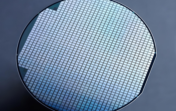
3. Semiconductor materials: from silicon to compounds
Material Type Typical Characteristics and Applications
Elemental semiconductor Silicon (Si) has a high crust content and is easy to process, and the core material of MOS devices
Germanium (Ge) Early device materials, now used in infrared optics
Compound semiconductor Gallium arsenide (GaAs) High electron mobility, suitable for high-frequency devices
Gallium nitride (GaN) wide bandgap, high voltage resistant, used for power electronics and LEDs
Key application scenarios:
Silicon-based devices: integrated circuits, solar cells (requires high purity silicon);
Compound semiconductors: lasers (GaAs), 5G communication devices (InP), electric vehicle power modules (SiC).
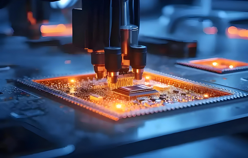
4. Integrated circuits: the ultimate form of semiconductors
Core component: transistor
Structure: a triode device composed of source, drain and gate;
Working principle: control the p-n junction carrier distribution through gate voltage to realize the current switching function;
Technology evolution: From planar transistors to FinFETs (3D structures), we continue to break through the limits of Moore's Law.
Manufacturing technology
Key steps: oxidation, photolithography, etching, ion implantation, metallization;
Technical Challenges:
Feature size reduced to nanoscale (such as 3nm process);
It is necessary to deal with physical restrictions such as quantum tunneling and thermal management;
Industry status: TSMC, Samsung and other companies have achieved mass production of processes below 5nm.
5. Future Outlook: Beyond Moore's Law
Technical direction
New device structure: GAA transistors and CFETs (complementary FETs) to improve integration;
New material system:
Two-dimensional materials (such as MoS?) realize atomic-level thickness transistors;
Superconducting materials explore zero resistance calculation;
Photoelectric fusion: Silicon photonic technology integrates optical communication and electronic computing.
Social impact
Computing power revolution: quantum computing and neuromimicry chips promote the development of AI;
Energy transformation: High-efficiency power devices support new energy vehicles and smart grids;
Biomedicine: Flexible electronic skin and implantable chips expand the medical boundaries.
Conclusion: The cornerstone of the scientific and technological revolution
Semiconductor technology is not only the core of electronic devices, but also a tool for humans to understand the world. From understanding the basic properties of matter to reconstructing the way society operates, every breakthrough in semiconductors is redefining "possible". Faced with challenges such as quantum effects and material limits, global scientific research forces are opening a new chapter in the "Post Moore era" through interdisciplinary collaboration.